
Diagram of the ZCU102 JTAG Chain
![]()
This post shows a block diagram of the Xilinx ZCU102 Evaluation Board’s JTAG chain.
Here is the JTAG chain on rev 1.0 and 1.1 of the ZCU102 as derived form the schematics:

Diagram available at [link]. A collection of just the JTAG connections available at [link].
From the ZCU102 Evaluation Board User Guide:
Vivado, SDK and or third-party tools (and PetaLinux Tools?) can establish a JTAG connection to the Zynq UltraScale+ MPSoC device through one of the three provided JTAG interfaces:
1. Xilinx platform USB or cable PC4 connector (J8)
2. ARM 20-pin JTAG connector (J6)
3. Digilent SMT2.5 USB-to-JTAG module with off-module micro-USB connector (J2)
Note: Only one of these connections can be used at a time.
If no FMC cards are installed, then the switches are closed and TDI can flow through to TDO as seen in this diagram from the JTAG Wiki:
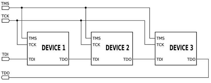
TDI (Test Data In)
TDO (Test Data Out)
TCK (Test Clock)
TMS (Test Mode Select)
TRST (Test Reset) optional
References
-
ZCU102 Evaluation Board User Guide UG1182 (v1.3) August 2, 2017 at [link]
-
ZCU102 Board Schematics (zcu102-schematic-source-rdf0403.zip) at [link] (sign-in required)
-
JTAG Wiki at [link]
-
Xilinx logo found via https://twitter.com/xilinxinc at [link]