
VHDL to Gates and Routing on an FPGA with Vivado
![]()
This post shows how to examine the gates and routing used to implement a VHDL design and set of constraints on the Zynq-7000 of a ZC706.
This post picks up right after [link]
Steps
Step 1: Examine the source for functionality
A) Click PROJECT MANAGER
B) Expand Design Sources (1)
C) Double-click buttonled(Behavioral) (buttonled.vhd)
D) Click on buttonled.vhd
D) Examine source
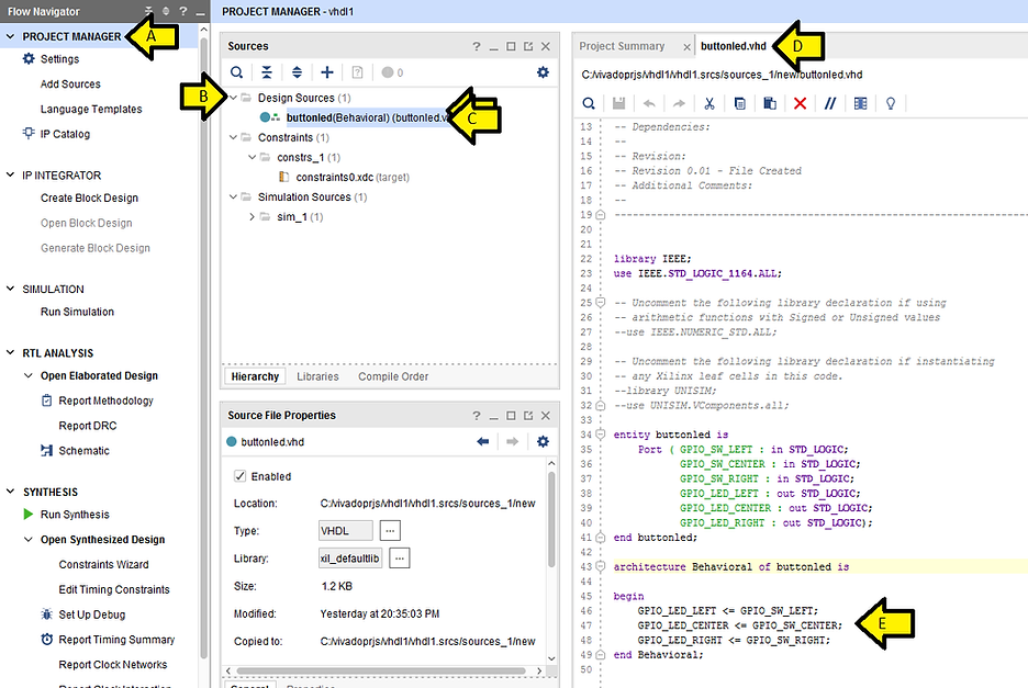
Here is the source in text:
Port ( GPIO_SW_LEFT : in STD_LOGIC; GPIO_SW_CENTER : in STD_LOGIC; GPIO_SW_RIGHT : in STD_LOGIC; GPIO_LED_LEFT : out STD_LOGIC; GPIO_LED_CENTER : out STD_LOGIC; GPIO_LED_RIGHT : out STD_LOGIC);
end buttonled;
architecture Behavioral of buttonled is
begin GPIO_LED_LEFT <= GPIO_SW_LEFT; GPIO_LED_CENTER <= GPIO_SW_CENTER; GPIO_LED_RIGHT <= GPIO_SW_RIGHT; end Behavioral;
Step 2: Examine the constraints for pin and drive strength assignments
A) Expand Constraints (1)
B) Expand constrs_1 (1)
C) Double-click constrints0.xdc (target)
D) Examine constraints
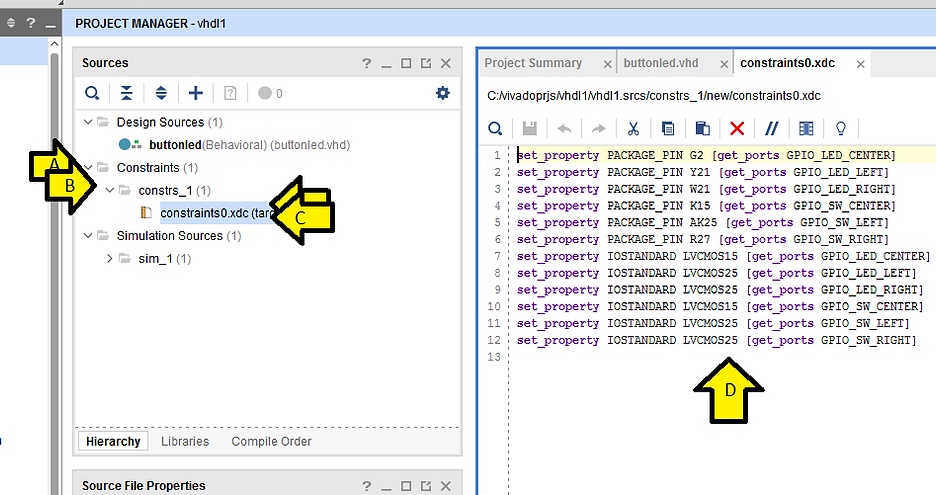
Here are the constraints in text:
set_property PACKAGE_PIN G2 [get_ports GPIO_LED_CENTER] set_property PACKAGE_PIN Y21 [get_ports GPIO_LED_LEFT] set_property PACKAGE_PIN W21 [get_ports GPIO_LED_RIGHT] set_property PACKAGE_PIN K15 [get_ports GPIO_SW_CENTER] set_property PACKAGE_PIN AK25 [get_ports GPIO_SW_LEFT] set_property PACKAGE_PIN R27 [get_ports GPIO_SW_RIGHT] set_property IOSTANDARD LVCMOS15 [get_ports GPIO_LED_CENTER] set_property IOSTANDARD LVCMOS25 [get_ports GPIO_LED_LEFT] set_property IOSTANDARD LVCMOS25 [get_ports GPIO_LED_RIGHT] set_property IOSTANDARD LVCMOS15 [get_ports GPIO_SW_CENTER] set_property IOSTANDARD LVCMOS25 [get_ports GPIO_SW_LEFT] set_property IOSTANDARD LVCMOS25 [get_ports GPIO_SW_RIGHT]
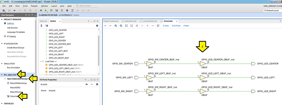
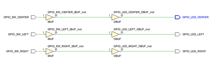
Step 3: Examine the schematic and device view for the entire buttonled.vhd circuit
A) Click on buttonled.vhd
B) Expand RTL ANALYSIS
C) Expand Open Elaborated Design
D) Click Schematic
E) Click on the white space above the schematic
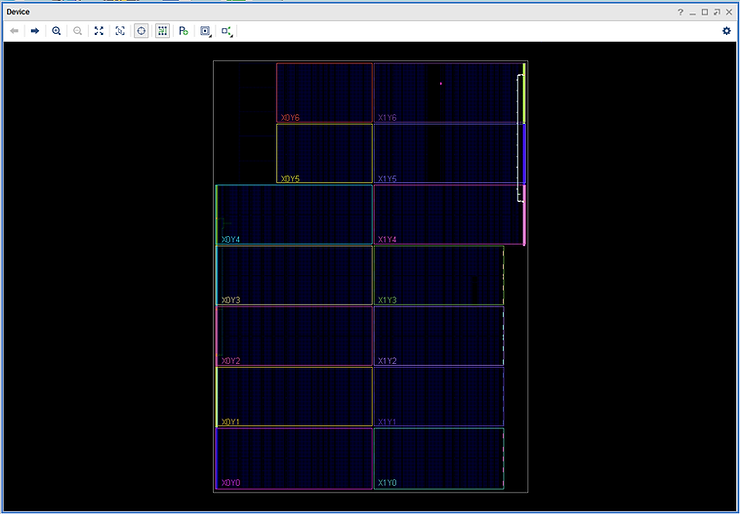
Step 4: Examine the Device view while in RTL ANALYSIS
A) Ensure you did Step 3 (make sure you clicked on the white space in the schematic view)
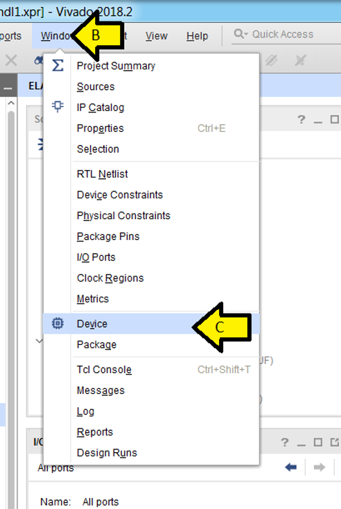
B) Click Window
C) Click Device
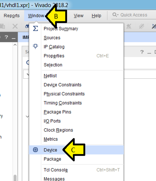
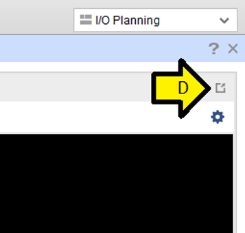
D) Click the Float icon
![]()
E) Place the Device window on a new screen
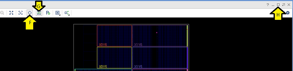
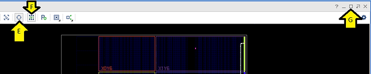
F) Click Auto-fit Selection so there’s a box around it
G) Click Routing Resources so there’s a box around it
H) Click Maximize
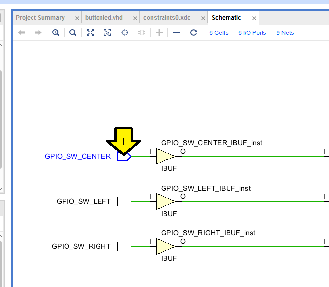
Now when you click on an element in the schematic, the Device window will automatically zoom there.
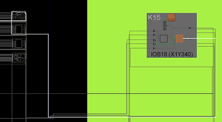
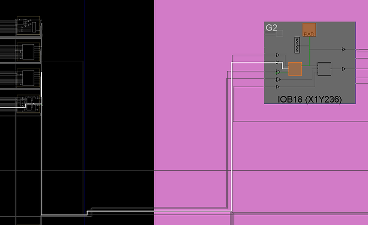
I) Click GPIO_SW_CENTER in the schematic
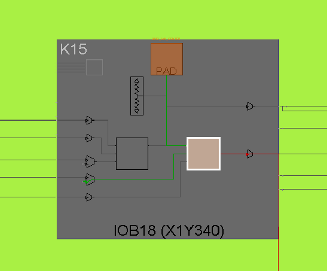
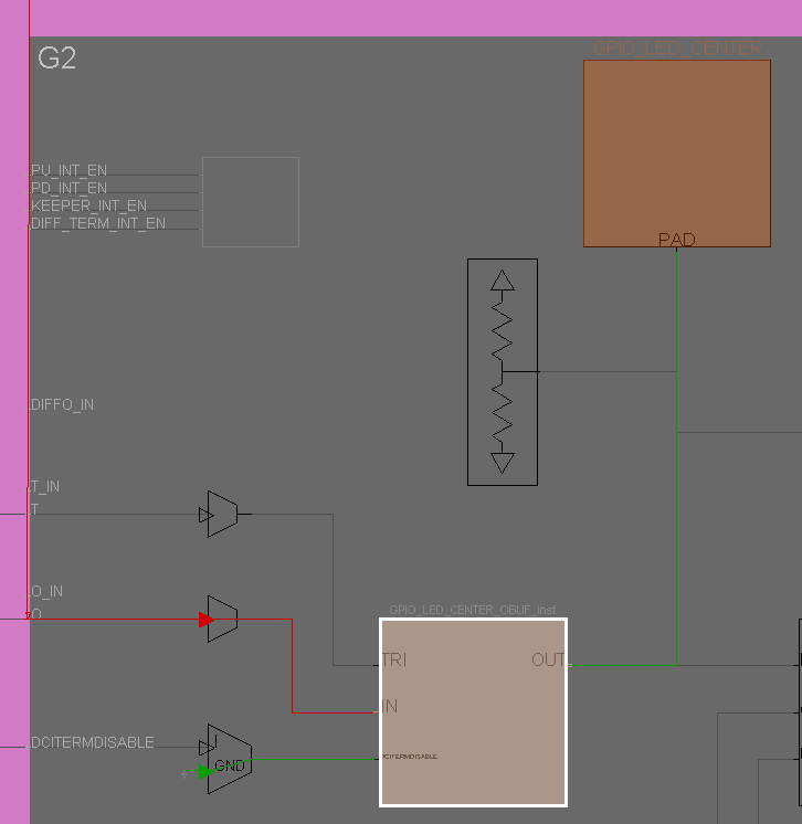
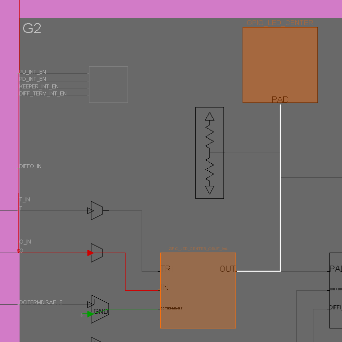
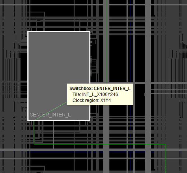
You should see the Device view jump to:
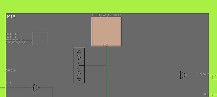
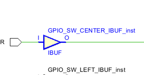
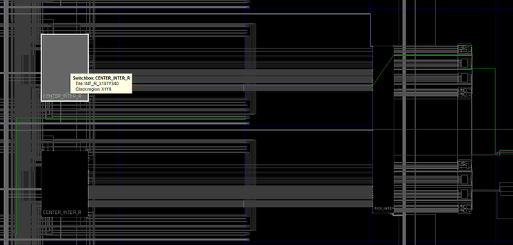
Note: this is the pad on K15 that GPIO_SW_CENTER maps to.
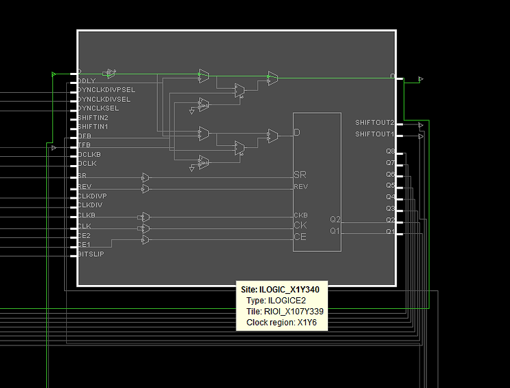
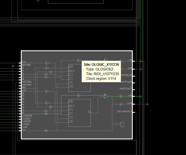
J) Click on the connection between GPIO_SW_CENTER and the I port of GPIO_SW_CENTER_IBUF_inst
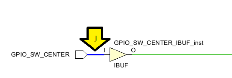
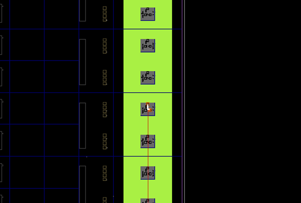
You should see the Device view jump to:
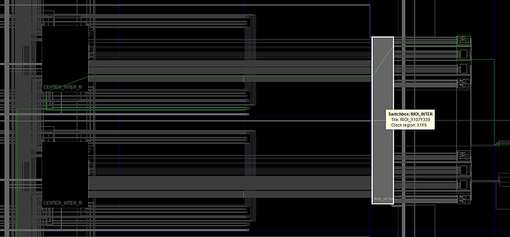
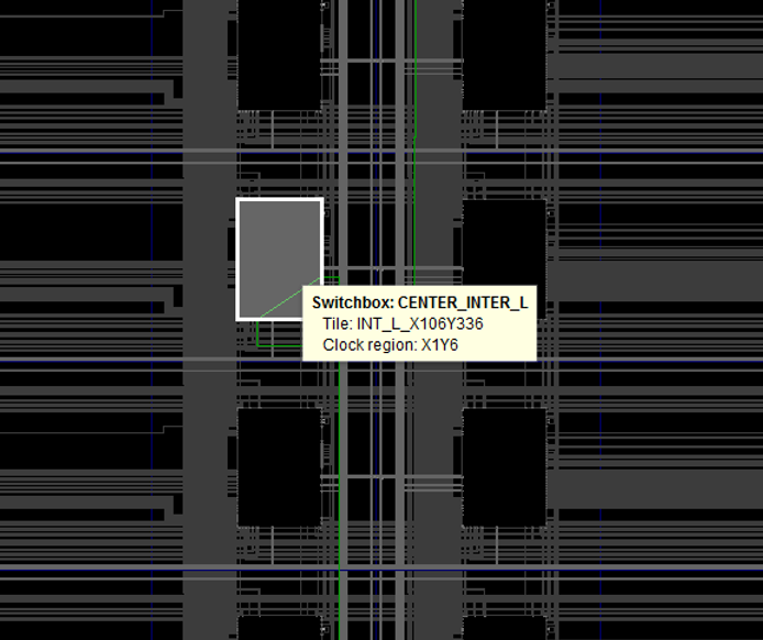
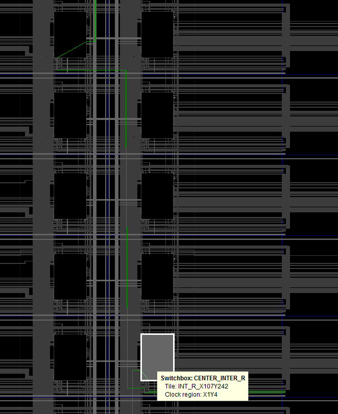
(K1) Click and drag (K2) to zoom in
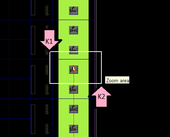
You should see:
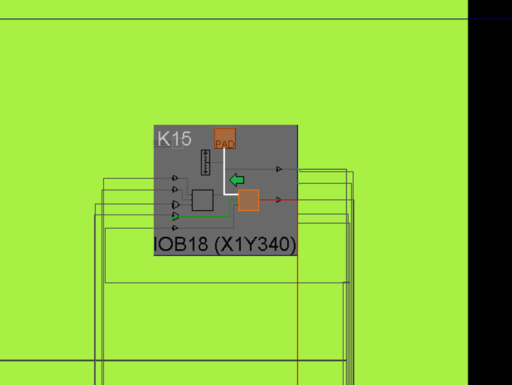
Notice the connection pointed at by the green arrow.
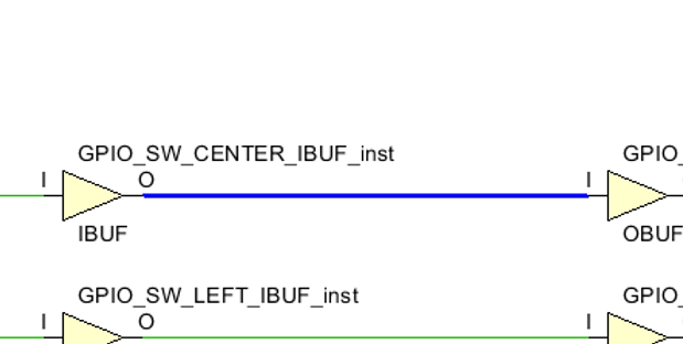
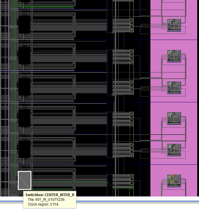
Here is the rest of the circuit in the RTL ANALYSIS view:
GPIO_SW_CENTER_IBUF_inst:
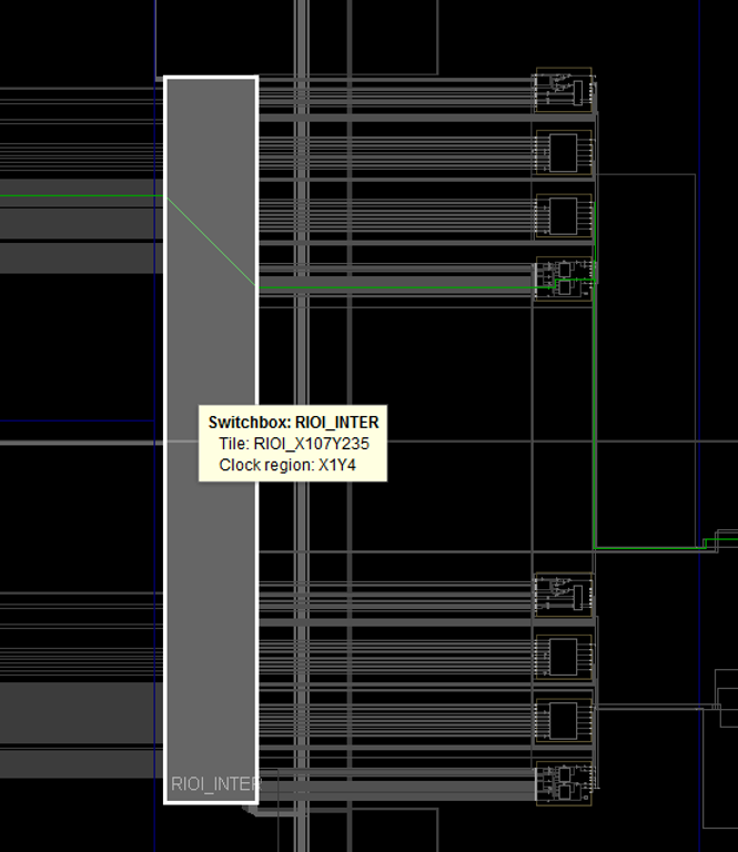
The connection between the O of GPIO_SW_CENTER_IBUF_inst and the I of GPIO_LED_CENTER_OBUF_inst:
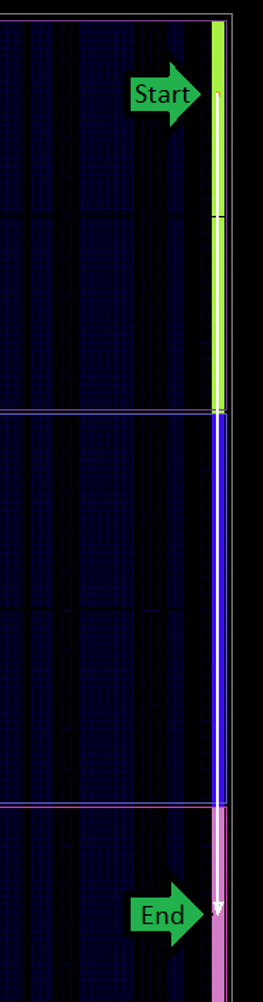
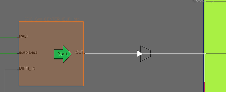
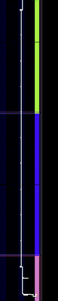
Zoomed in at Start:
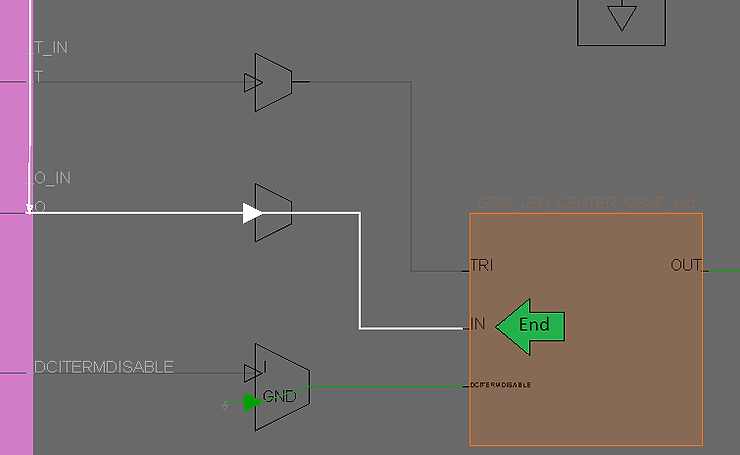
Zoomed in at the End:
GPIO_LED_CENTER_OBUF_inst
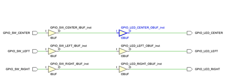
The connection between the O of GPIO_LED_CENTER_OBUF_inst and GPIO_LED_CENTER:
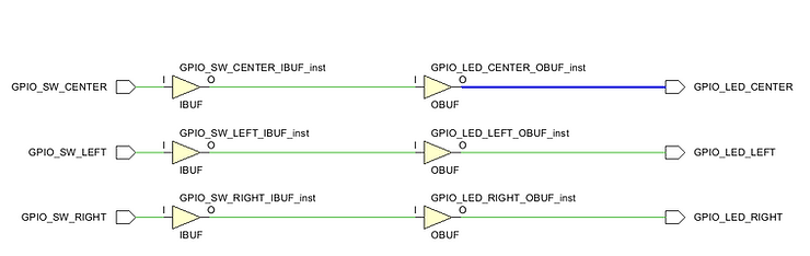
…and GPIO_LED_CENTER:
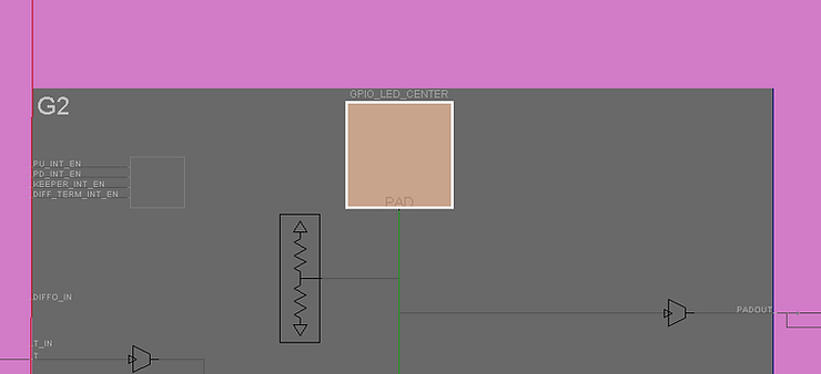
Step 5: Examine the Device view while in IMPLEMENTATION
Note: you will see all the routing in this view
A) Click IMPLEMENTATION
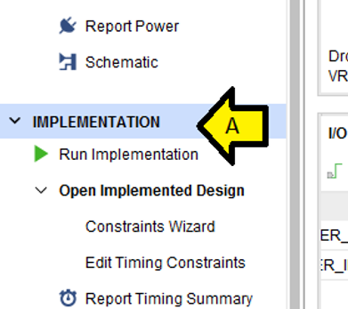
B) Click Window
C) Click Device
D) Click Float
E) Place the Device window on a new screen
F) Click Auto-fit Selection so there’s a box around it
G) Click Routing Resources so there’s a box around it
H) Click Maximize
You should see:
Here is the actual routing:


…then travel down:
…to the end:
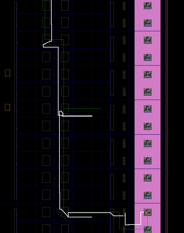


…and finaly
Reference
- Xilinx logo from https://twitter.com/xilinxinc